MAX262 Programmable Filter Bandpass Band-Resistant All-Pass Low-Pass High-Pass
Tax included.
Overview:
The LP/HP/BP/NO filter can be built using the principle of switched capacitor filtering.
The internal contains two identical filtering units A/B, each unit is two-section filtering, so a MAX262 can form a fourth-order filter.
Four parameters are used when using: center frequency f0, Q value, clock frequency, working mode. The type of filter (LP/HP/BP/NOTCH) is determined by the pin connection. The cutoff frequency f0 of the filter is determined by fclk and the parameter FN. The Q value of the filter is determined by the parameter QN.
The parameter measurement can be more accurate, but because it is switched capacitor filtering, so the output waveform is stepped. The common method is to add a RC low-pass filter to remove the high-frequency clock signal.
Detailed Description:
1. Four modes
Mode 1: Band pass, low pass. Applicable types Butterworth, Chebyshev, Bessel. Can also be used for band stop filters.
Mode 2: All-pole band pass, low pass
Mode 3: Elliptical Bandpass, Elliptical Lowpass, Qualcomm
Mode 4: All Pass
2. Fclk is input through pin CLKA/CLKB, which can change the cutoff frequency of the filter together with the parameter FN.
3. The FN value is a decimal representation of the binary value for F0,Q.
The center frequency range is 1HZ-100KHZ, and the MAX262 center frequency can be up to 140KHZ.
Calculation method of center frequency or inflection point frequency:
Mode 1, 3, 4: Fclk / f0 = (26 + N) pi / 2; converted f0 = fclk * 2 / pi / (26 + N)
Mode 2: N= fclk/f0/1.11072-26·
4. QN values ?����range from 0.5-64.0, maximum mode up to 90
Q value control word calculation method:
Mode 1, 3, 4: N = 128-64/Q
Mode 2: N=128-90.51/Q
5. The working mode, FN, and QN can be stored in the MAX262 internal ROM by writing the address lines, data lines, and control lines of the MAX262, thereby making the system work.
Select A0-A3, the data in the ROM will be updated, and D0/D1 for the data bits. Data is written on the rising edge of the WR signal. The electrical signal at the Fclk input does not interfere with the digital signal.
Detail:
1. Adding a latch/trigger to the SCM when connected to the MAX262 can significantly reduce interference.
2. There are two ways to set the frequency f0:
Method 1: fclk is fixed and the value of FN is changed. Since the FN range is only [0-63], the step value is small and the accuracy is low.
Method 2: FN is fixed and fclk is changed. Adjusting fclk gives a satisfactory cutoff frequency.
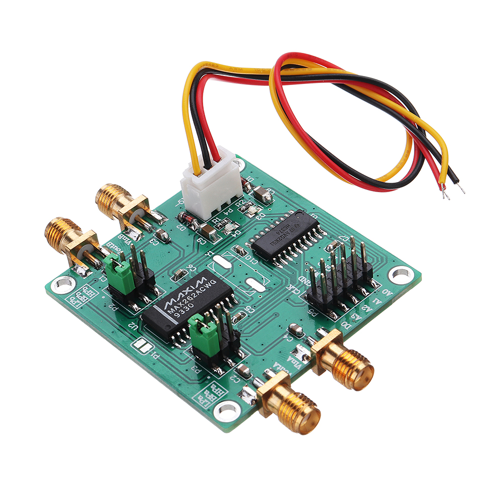
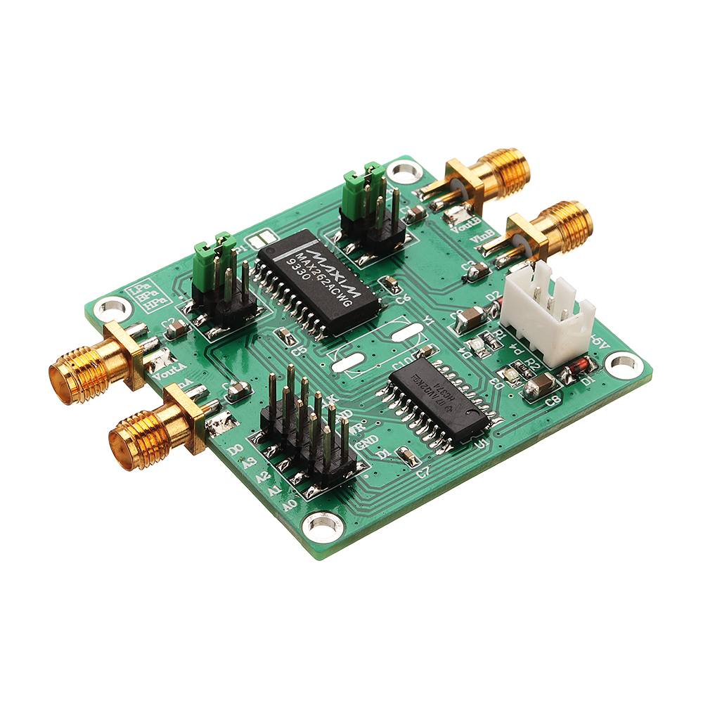
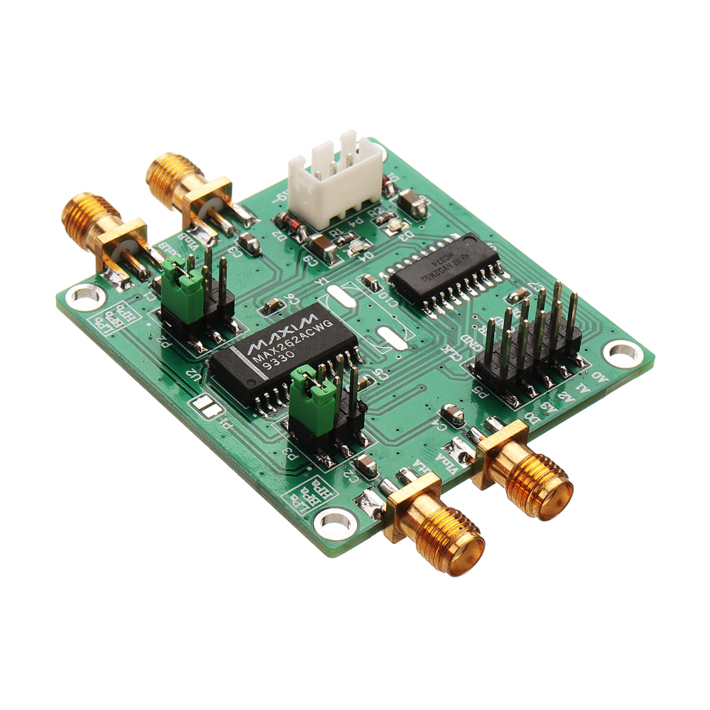
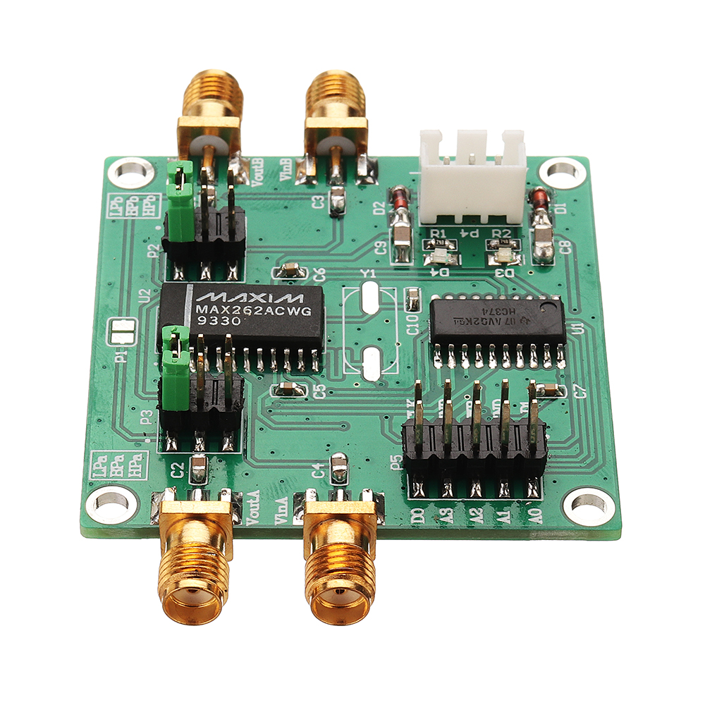
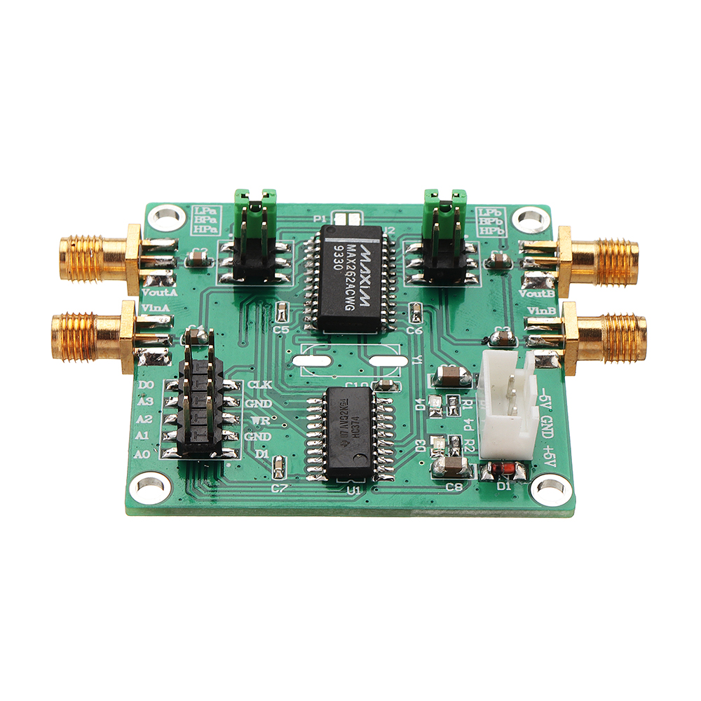
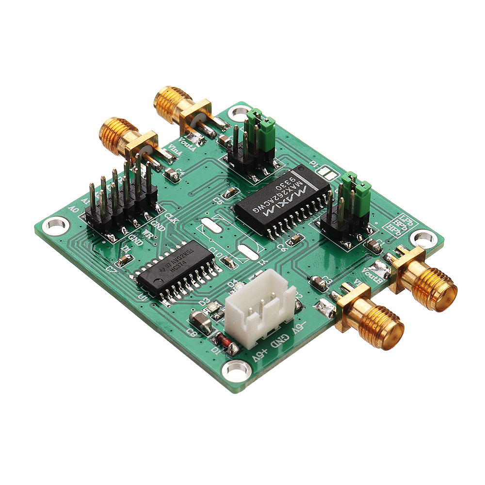
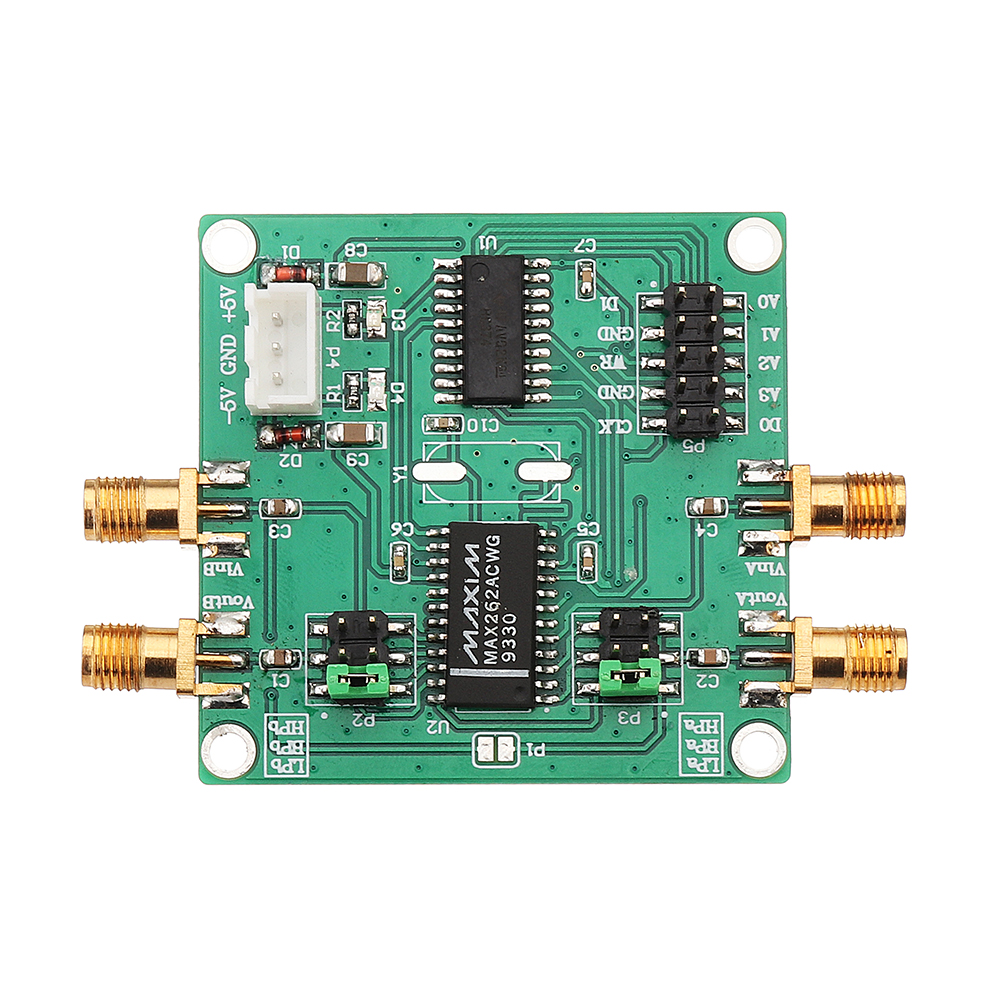
Features:
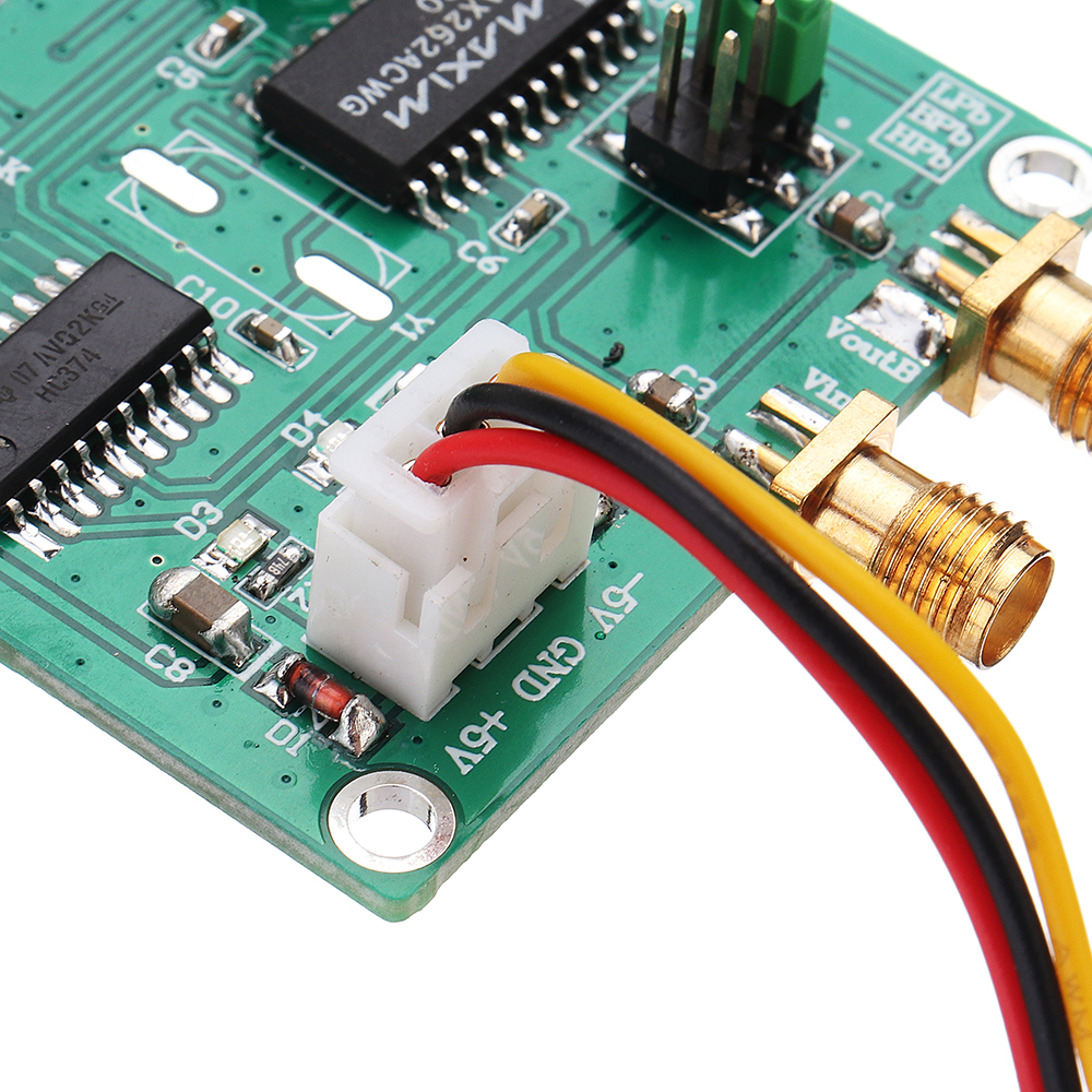
1. Power: ±5V typical power supply
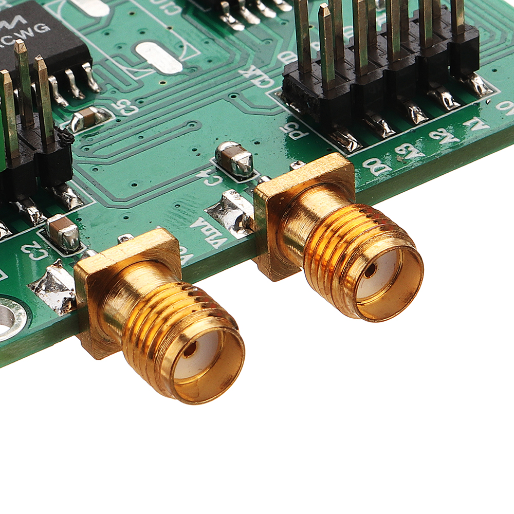
2. Input and output two SMA interfaces INA, INB, VOUTA, VOUTB, output A and B can be cascaded by jumper P1 to realize fourth-order or other form of filter
Package includes:
1 x MAX262 Programmable Filter